Demo
Upload a layout, find narrow features, and inspect the patterns that deserve a closer look.
Explore a public layout
Find candidate locations and inspect their local shapes in the live demo.
Try Live DemoUse non-confidential files only. The free server may take time to wake up and process an analysis.
Start with locations and patterns. GeoSignal screens the selected GDS layer for narrow widths and gaps, then calculates optical images for a limited set of candidates. Focus / Dose comparison is an optional next step.
1. Screen guide
The proposed screen below starts with a layout overview and six candidates per type by default. Choose 4, 6 or 8, switch between Width and Space, and click a pattern to see it at full width below. Candidate count controls detailed review; it does not limit geometry detection.
This is an interactive, saved-data preview, not a live analysis session. Six examples per type are available. Actual PW data is available for Width #1 and Space #1; the other cards show an uncalculated state. Choosing 8 does not invent additional examples. The deployed app may still show the previous interface.
| No. | Item | How to use it |
|---|---|---|
| ① | File | Choose a public, non-confidential GDS/OAS file. |
| ② | Layer / Datatype | Select the target layer. TT04 PWM 68/20 can also be reviewed. |
| ③ | Width / Space limit | Geometry screening limits, not printed-CD tolerances. |
| ④ | ROI / Pixel size | Review area and pixel spacing. Illumination stays at dense7. |
| ⑤ | Focus / Dose | Enter symmetric ranges. Compare shapes and CD changes at nine combinations. |
| ⑥ | Override reference | Usually leave blank. To fit another design reference, enter its center X/Y, design width and measurement direction. |
| ⑦ | Candidate locations | Locate candidate regions across the GDS. |
| ⑧ | Main candidates | Default: 6 per type; choose 4 / 6 / 8. Click a card for a full-width detail image. |
| ⑨ | Optional comparison | Expand the selected candidate’s 3×3 images and Bossung curve. No pass/fail grading. |
Using the live demo
The screen above previews the updated workflow. In the currently deployed app, files outside the registered examples may still require an explicit reference location, direction and design width. Follow the reference fields shown in that app.
Usually, leave Override reference blank. These examples share the TT04 PWM 67/20 anchor at (147.770, 108.460) µm, fitted to its 170 nm design width. This is a common comparison baseline, not calibration to measured wafers. Other patterns are not individually fitted.
2. Find the main candidates
The overview locates candidates across TT04 PWM 67/20. Markers identify places to inspect, not confirmed manufacturing defects.
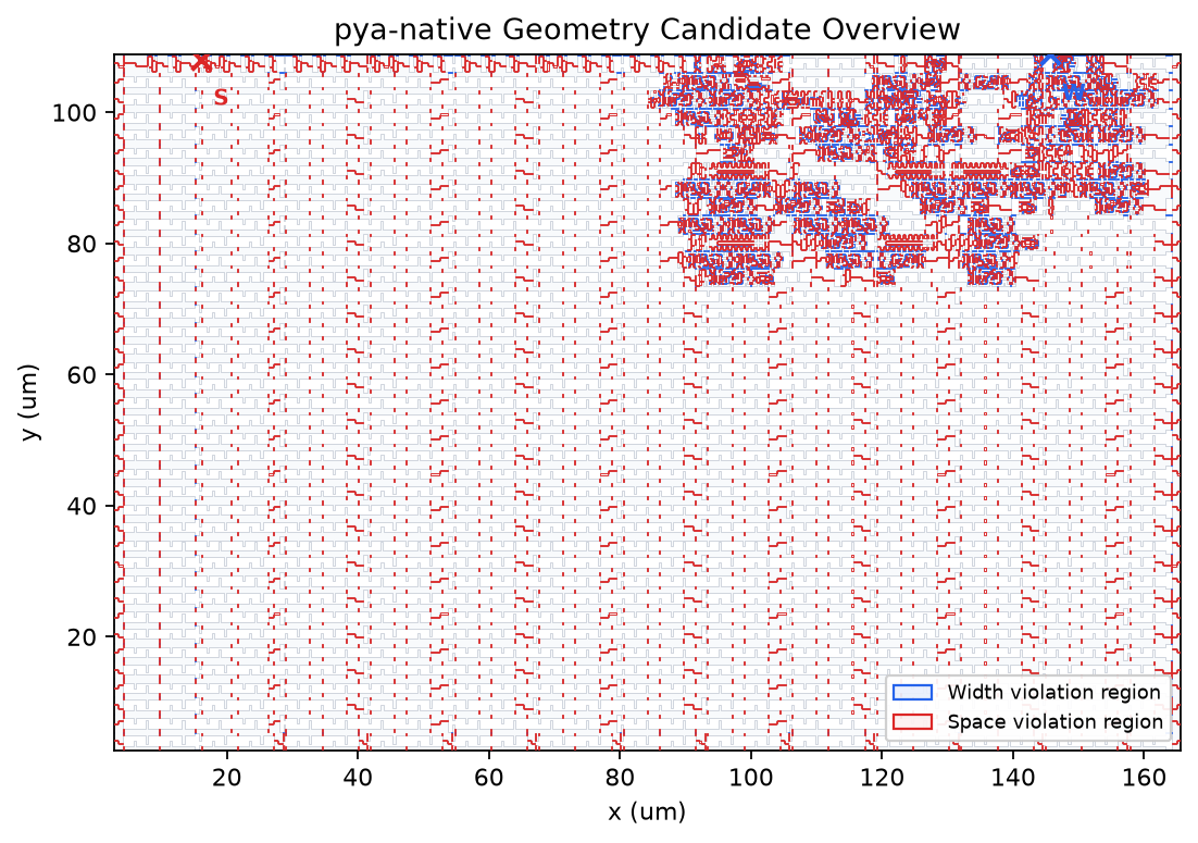
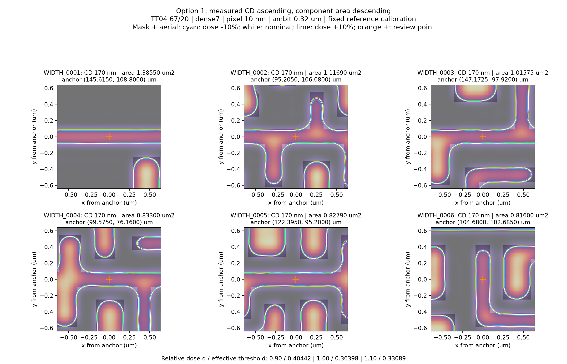
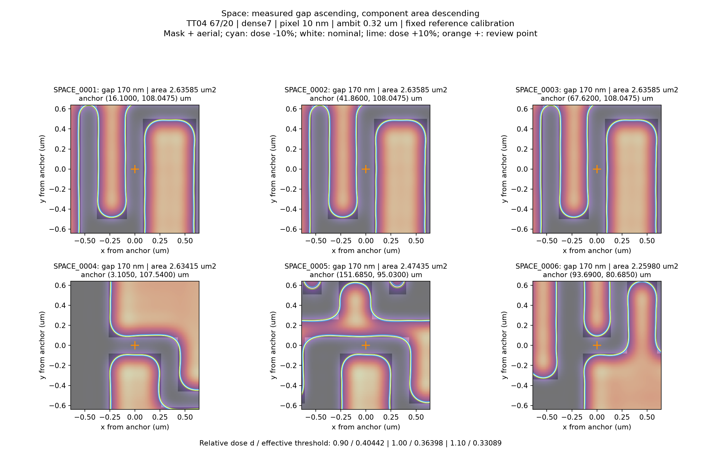
Narrower geometry comes first; ties prefer larger candidate regions. The galleries below show six Width and six Space examples. Warm colors show light intensity; cyan, white and lime contours represent dose −10%, nominal and +10%.
Image scale: Candidate close-ups (including nominal and 3×3 images) show a 1.28 × 1.28 µm zoom inside a 2.56 × 2.56 µm calculation ROI. The calculation also includes a 0.32 µm optical margin on each side. Zooming changes only the displayed area, not the calculation conditions. The layout overview shows the full layer.
Width · top 6
Space · top 6
3. Actual examples: 67/20 and 68/20
These are actual local calculations on the public TT04 PWM GDS, using the same 67/20 reference. Each example keeps its candidate and measurement location fixed. They are not Render runtime tests or a ranking of entire layers.
Start with the nominal pattern pair. Open the optional comparison to see nine conditions and the corresponding Bossung curves.
The examples below use the same 1.28 µm zoom and 2.56 µm calculation ROI.
TT04 PWM 67/20
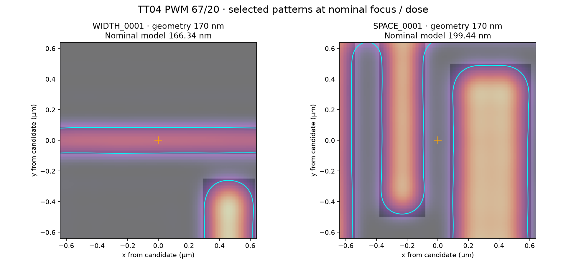
The geometry and model measurements differ because the common reference is not fitted separately to these candidates.
Optional: Focus / Dose images and Bossung curves
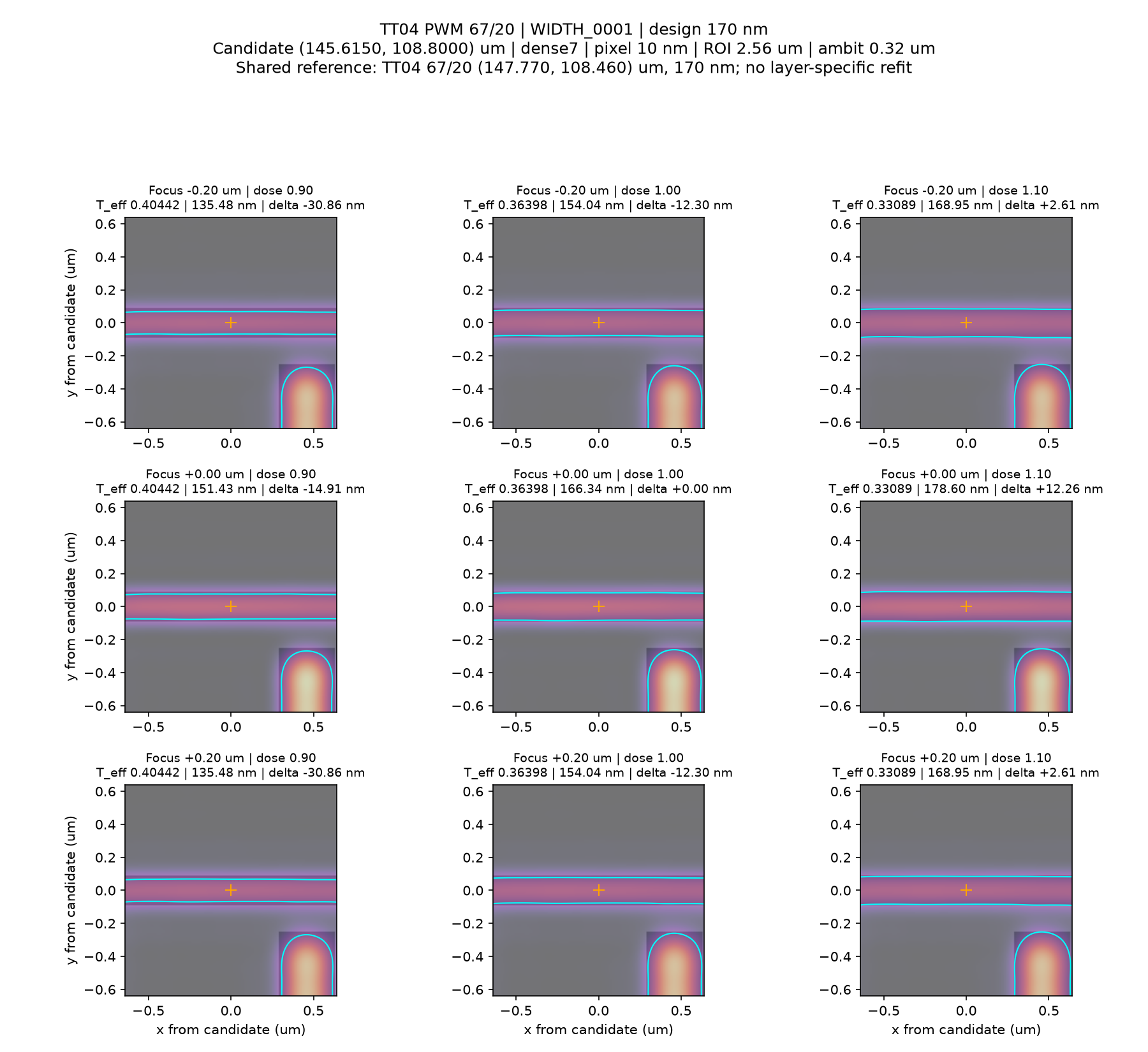
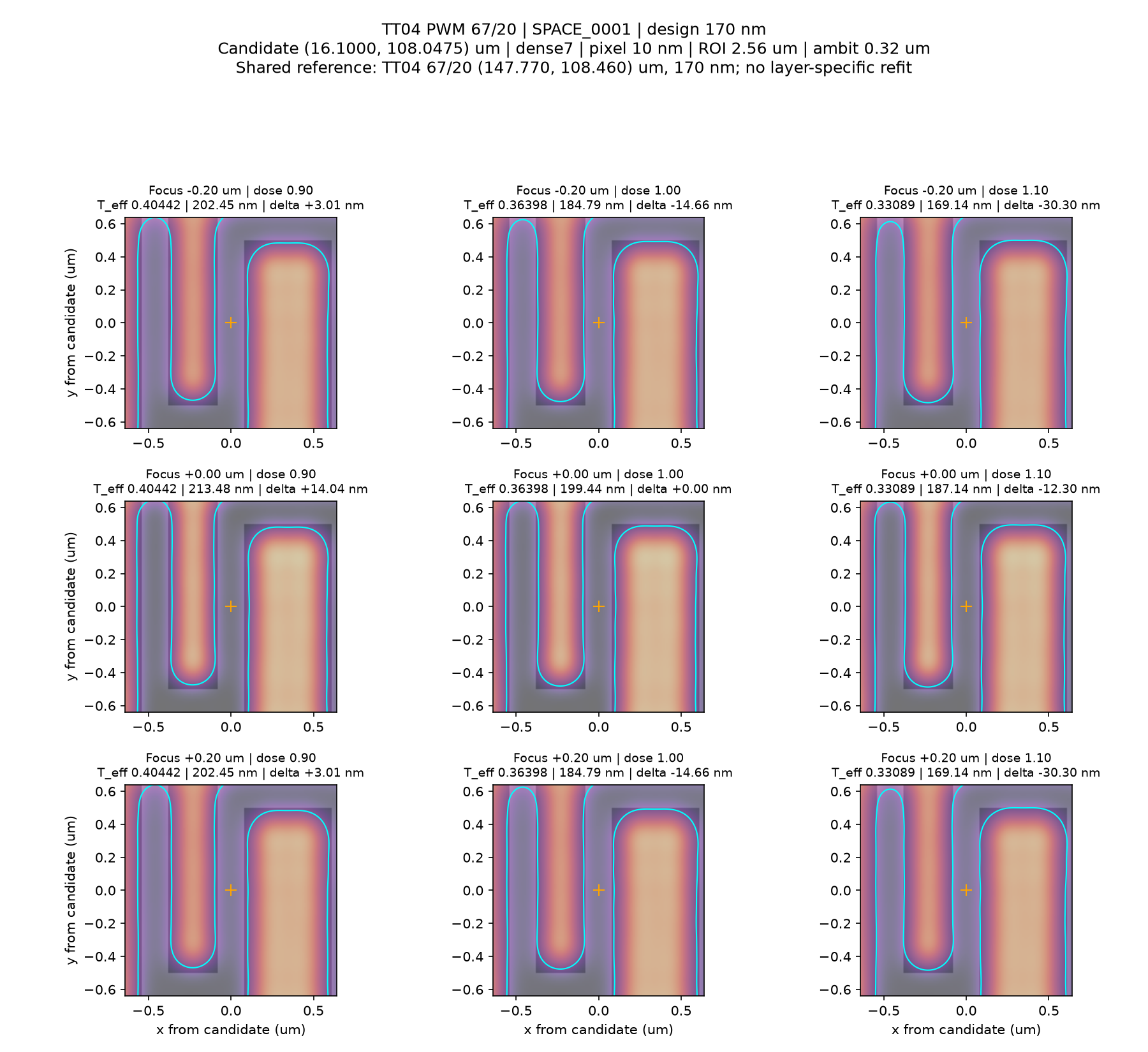
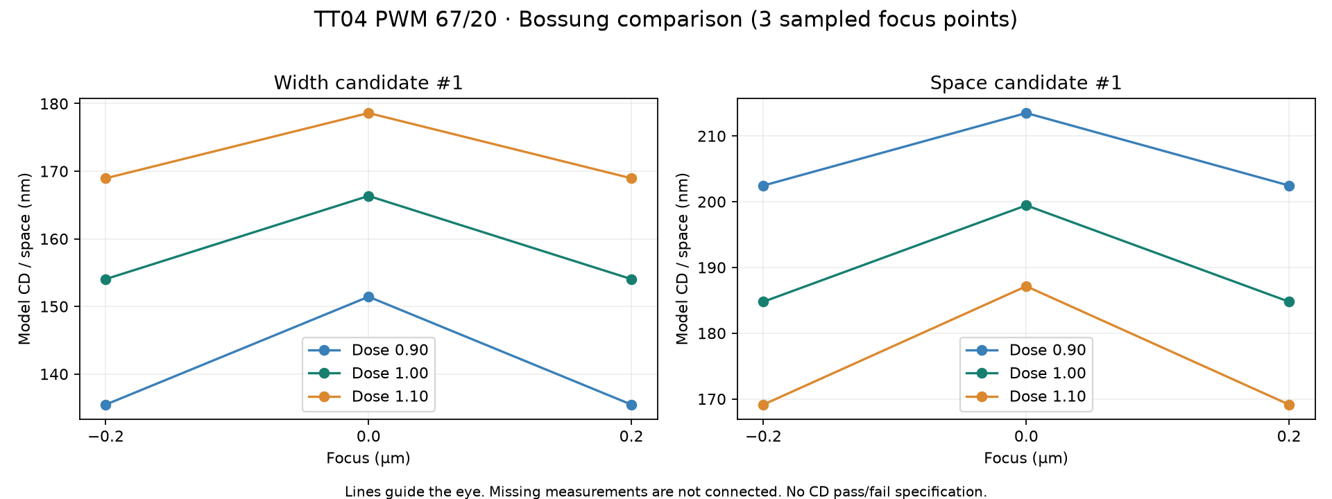
Focus: −0.20 / 0 / +0.20 µm. Relative dose: 0.90 / 1.00 / 1.10. Bossung plots show measured size against focus, one line per dose. Missing measurements are not connected; three sampled points show a trend, not a precise DoF estimate. No CD pass/fail specification is applied.
TT04 PWM 68/20
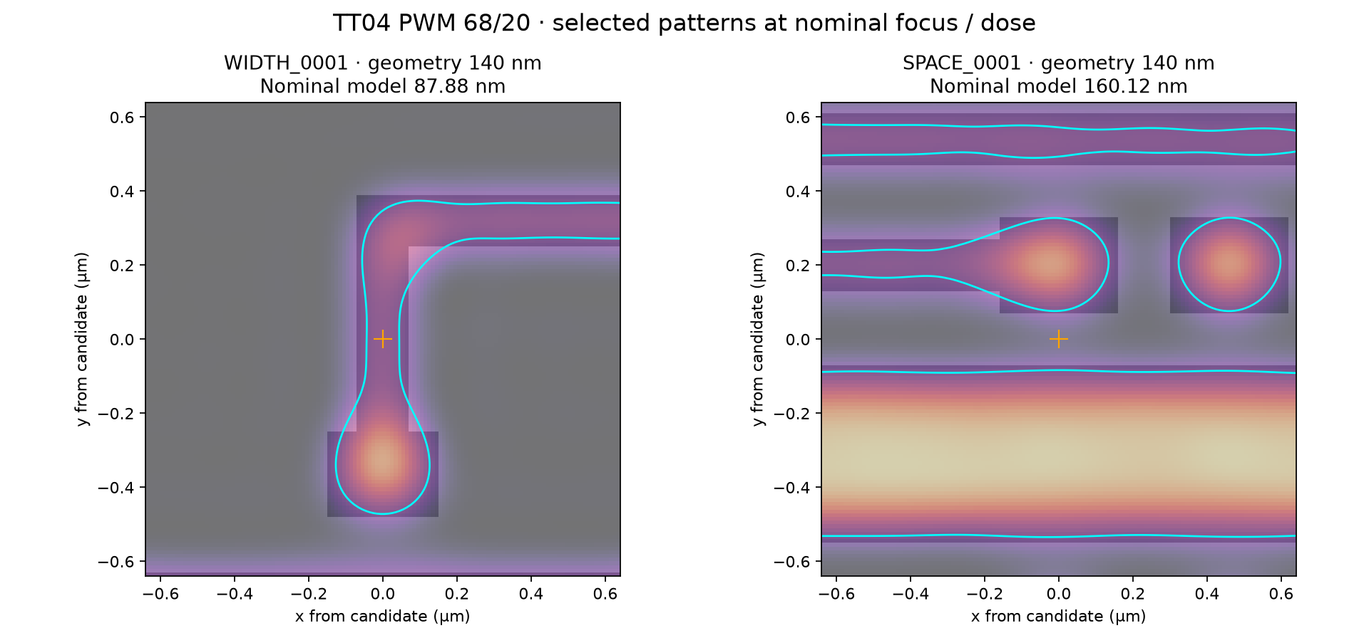
The selected width candidate has a narrow neck. Its nominal model width is about 88 nm versus 140 nm in the geometry. At dose 0.90 and focus ±0.20 µm, the fixed-gauge measurement reports a missing feature. This is a local model response, not a wafer-defect claim.
Optional: Focus / Dose images and Bossung curves
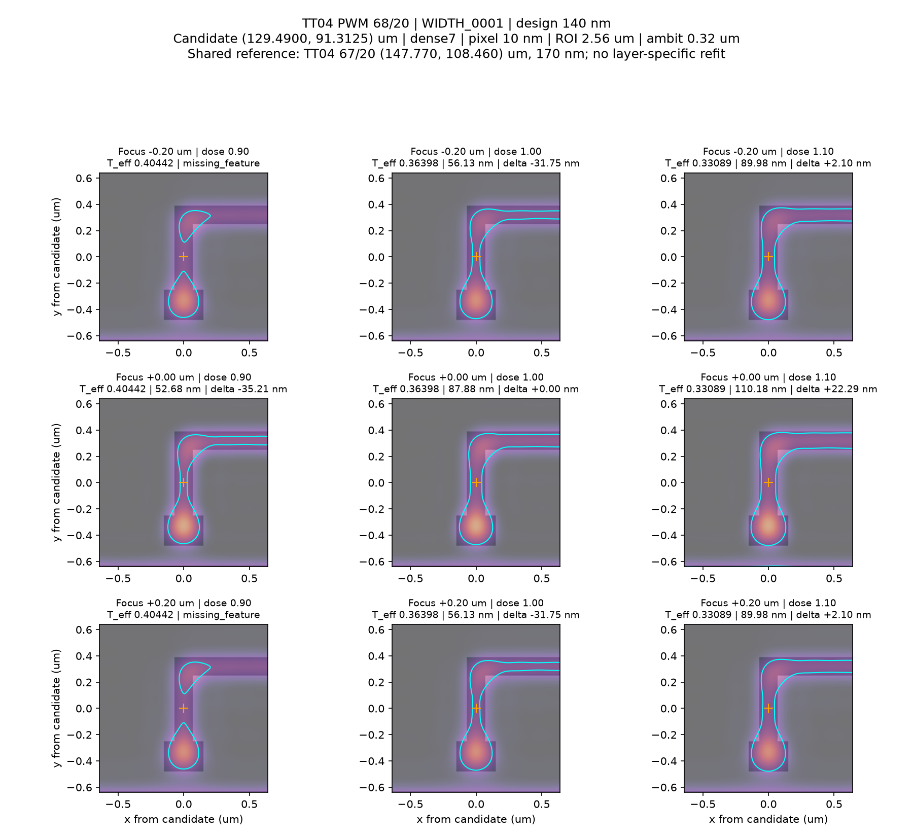
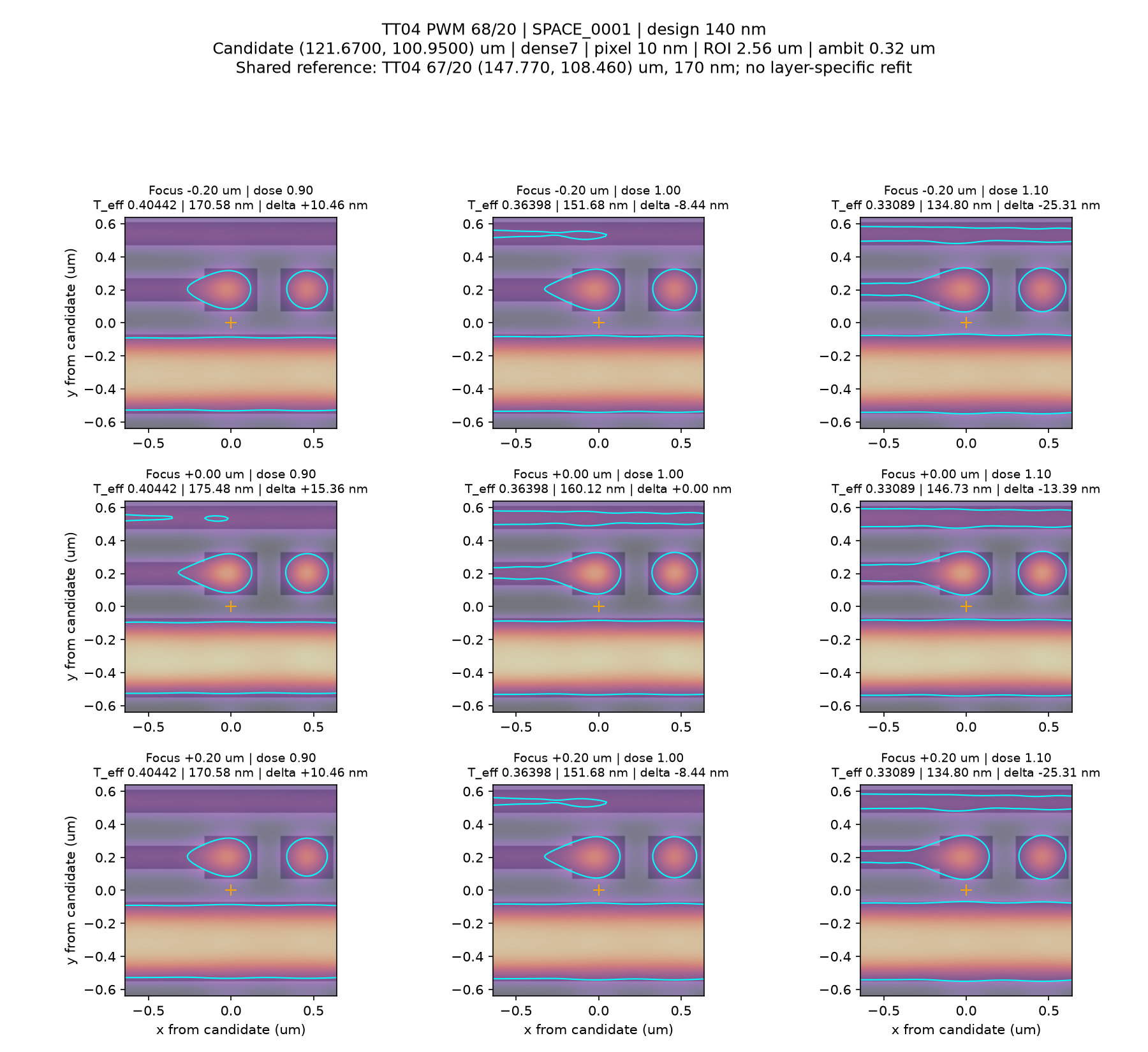
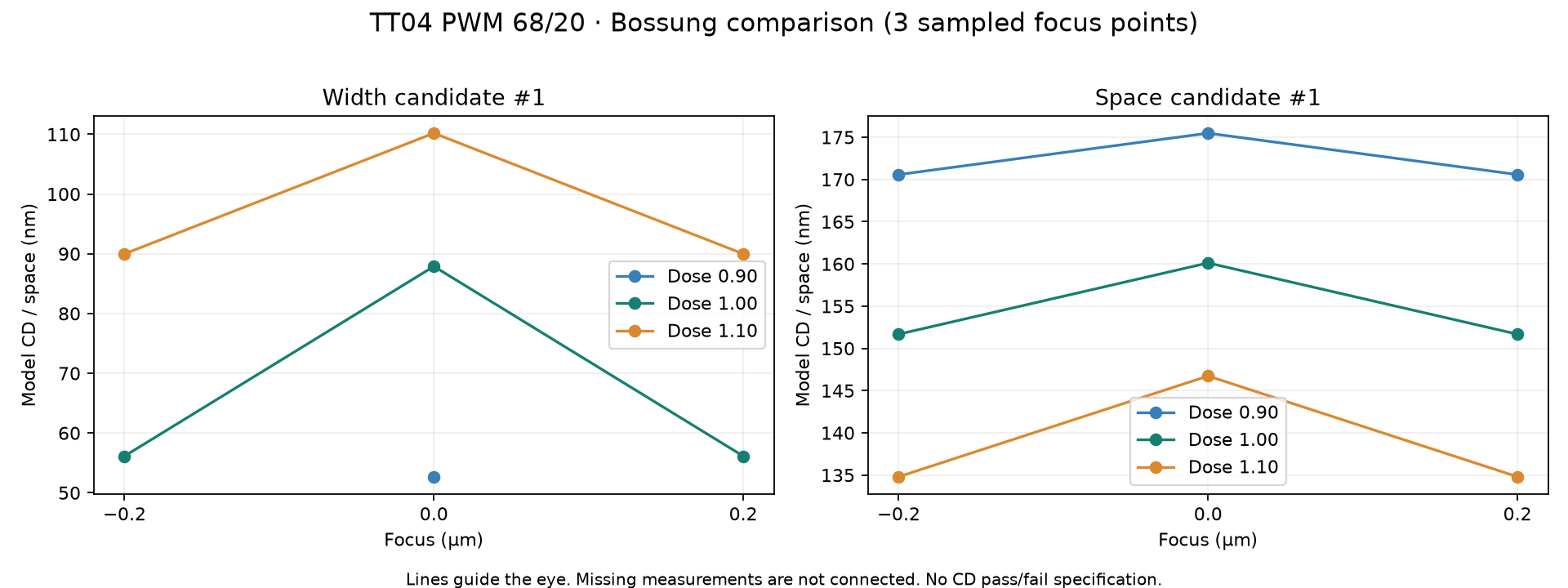
Focus: −0.20 / 0 / +0.20 µm. Relative dose: 0.90 / 1.00 / 1.10. Bossung plots show measured size against focus, one line per dose. Missing measurements are not connected; three sampled points show a trend, not a precise DoF estimate. No CD pass/fail specification is applied.
4. Read the results
Look for a narrowing neck, a closing gap, rounded corners or a line end pulling back. The orange cross marks the measurement location. In the 3×3 images, cyan marks the calculated contour and Δ shows the change from that candidate’s nominal result. Brightness is held consistent within each comparison.
The model treats polygons as illuminated regions. These contours do not determine which material remains after resist development or etch. They are relative model results for study, not calibrated process predictions.
5. Data and details
The review GDS is the saved 67/20 example; it does not include the 68/20 comparison. Upload only public, non-confidential layouts.